


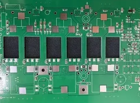
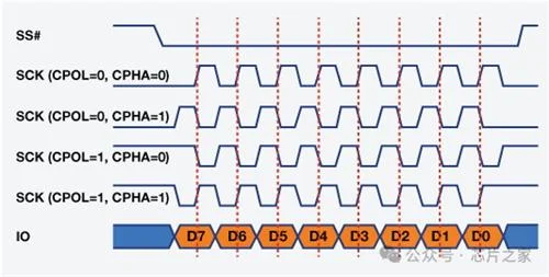
Communication Process of I2C, SPI, and UART Protocol
I2C, SPI, and UART remain the most commonly used communication protocols in embedded electronic devices. In this article, we will delve into these
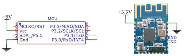
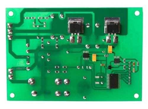
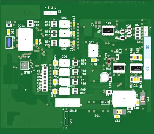
Communication Level Conversion Circuit Ideas
Communication level conversion is essential when integrating electronic devices with different operating voltage levels. This article explores various circuit ideas for achieving seamless
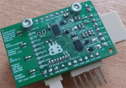
Firmware Extract: What Is The Original Program Code?
The original programmed code on an integrated circuit (IC) refers to the firmware or software that is embedded within the IC’s memory and
What Is BIN File, and How Are They Used?
A BIN file, short for “binary file,” is a type of file format that stores data in binary form. This means that the
"I needed a PCB reverse engineering project completed on a tight timeline, and PCBDesign Lab delivered beyond my expectations. They were able to accurately reverse engineer the circuitry and provide me with detailed schematics and PCB files in a timely manner. I would highly recommend their services to anyone in need of PCB reverse engineering."

Mr. Justin
"I had a complex PCB design project that required a high degree of customization, and PCBDesign Lab was able to deliver exactly what I needed. Their team worked closely with me to understand my project requirements and provided me with a PCB design that exceeded my expectations."

Mr. Enrique Guzmán
"I was impressed with the PCB design services provided by PCBDesign Lab. They were able to take my initial concept and turn it into a functional and efficient design. Their attention to detail and dedication to quality is truly unmatched in the industry."

Mr. Johnell Gallemit